- 您现在的位置:买卖IC网 > Sheet目录114587 > 552CC000230BGR (SILICON LABORATORIES) VCXO, CLOCK, 24.576 MHz, CMOS OUTPUT
Si552
6
Rev. 0.5
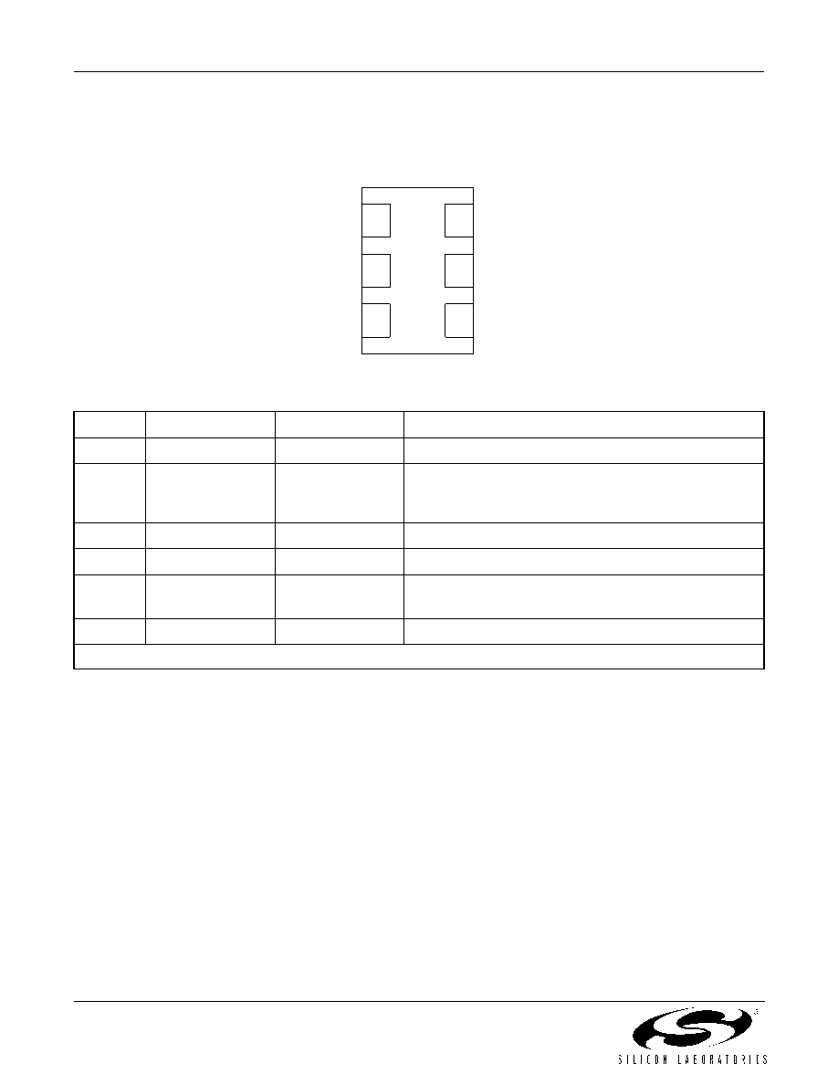
2. Pin Descriptions
Table 10. Si552 Pin Descriptions
Pin
Name
Type
Function
1
VC
Analog Input
Control Voltage
2
FS*
Input
Frequency Select:
0 = first frequency selected
1 = second frequency selected
3
GND
Ground
Electrical and Case Ground
4
CLK+
Output
Oscillator Output
5
CLK–
(N/A for CMOS)
Output
Complementary Output
(N/C for CMOS)
6
VDD
Power
Power Supply Voltage
*Note: FS includes a 17 k
1
2
3
6
5
4
VC
GND
FS
VDD
CLK+
CLK–
(Top View)
发布紧急采购,3分钟左右您将得到回复。
相关PDF资料
552AD000127BG
VCXO, CLOCK, 693.48299 MHz, LVPECL OUTPUT
550AC250M000BGR
VCXO, CLOCK, 250 MHz, LVPECL OUTPUT
550AD669M327BGR
VCXO, CLOCK, 669.327 MHz, LVPECL OUTPUT
552AC000189BGR
VCXO, CLOCK, 126.2 MHz, LVPECL OUTPUT
554CD000010BGR
VCXO, CLOCK, 108 MHz, CMOS OUTPUT
554CD000110BGR
VCXO, CLOCK, 108 MHz, CMOS OUTPUT
550AD216M000BGR
VCXO, CLOCK, 216 MHz, LVPECL OUTPUT
554MD000244BG
VCXO, CLOCK, 166.6286 MHz, LVPECL OUTPUT
相关代理商/技术参数
552CC000230DG
功能描述:VCXO振荡器 DUAL VCXO 6 PIN 0.5PS RS JTR RoHS:否 制造商:Fox 封装 / 箱体:5 mm x 3.2 mm 频率:19.2 Mhz 频率稳定性:2.5 PPM 输出格式: 封装:Reel 电源电压:3 V 端接类型:SMD/SMT 尺寸:3.2 mm W x 5 mm L x 1.5 mm H 最小工作温度:- 20 C 最大工作温度:+ 75 C
552CC000353DG
功能描述:VCXO振荡器 DUAL VCXO 6PIN .5ps RMS jitter RoHS:否 制造商:Fox 封装 / 箱体:5 mm x 3.2 mm 频率:19.2 Mhz 频率稳定性:2.5 PPM 输出格式: 封装:Reel 电源电压:3 V 端接类型:SMD/SMT 尺寸:3.2 mm W x 5 mm L x 1.5 mm H 最小工作温度:- 20 C 最大工作温度:+ 75 C
552CC000432DG
功能描述:VCXO振荡器 DUAL VCXO 6PIN .5ps RMS jitter RoHS:否 制造商:Fox 封装 / 箱体:5 mm x 3.2 mm 频率:19.2 Mhz 频率稳定性:2.5 PPM 输出格式: 封装:Reel 电源电压:3 V 端接类型:SMD/SMT 尺寸:3.2 mm W x 5 mm L x 1.5 mm H 最小工作温度:- 20 C 最大工作温度:+ 75 C
552CC622M080BG
制造商:SILABS 制造商全称:SILABS 功能描述:DUAL FREQUENCY VCXO (10 MHZ TO 1.4 GHZ)
552CC622M080BGR
制造商:SILABS 制造商全称:SILABS 功能描述:DUAL FREQUENCY VCXO (10 MHZ TO 1.4 GHZ)
552CD000109DG
制造商:Silicon Laboratories Inc 功能描述:CNTRLD OSC 74.175824MHZ/74.25MHZ VCXO CMOS 6PIN - Trays
552CD000131DG
制造商:Silicon Laboratories Inc 功能描述:OSCILLATOR - Trays
552CD000131DGR
制造商:Silicon Laboratories Inc 功能描述:OSCILLATOR - Tape and Reel